This article is more than 1 year old
The 3D die stack tack: Toshiba builds towering column of flash
Resistance is futile
Toshiba is building high rise flash and ReRAM chips, with prototypes coming next year and volume shipping in 2015.
The idea of high-rise or 3D chips is that we can sidestep limitations on increasing the storage density of flash or memory chips by stacking them one on top of the other, increasing the storage density on a Mbits/in 2 basis by building upwards, in the same way as high-rise housing increases the number of people living in the ground footprint of a block of flats.
Hot on the heels of our story about the NAND scaling trap, with 3D NAND and ReRAM suggested as two of the potential escape routes, we learn from Nikkei Electronics that Toshiba is building 3D dies using a type of NAND, its p-BiCS (pipe-shaped Bit Cost Scalable) technology, and also a coming replacement technology for NAND, ReRAM (Resistive RAM) which combines attributes of RAM and NAND to provide byte addressability, DRAM-class speed and NAND non-volatility.
As the slide below shows, 3D flash involves layers of NAND dies with communicating holes - TSVs or Through Silicon Vias - linking them to a stack controller at the base of the stack. It is not stacking NAND chips one atop the other but rather stacking layers of NAND in a single chip.
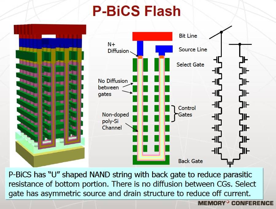
Toshiba p-BiCS technology
Toshiba's p-BiCS NAND has a 50nm-size hole and 16 layers. Toshiba's chief engineer, Masaki Momodomi, at its Semiconductor & Storage Products Co., says that p-BiCS becomes cheaper than ordinary NAND when more than 15 layers are used, presumably comparing similar capacity levels. The company aims to deliver 128Gbit and 256Gbit prototype samples next year, engineering samples in 2014, with volume shipments in 2015; we are more than two years away from seeing product hit the streets.
The ReRAM technology has a similar timescale though at lower capacities. It has much faster write times than NAND and Toshiba sees it fulfilling a different role from p-BiCS, being used closer to CPUs than p-BiCS, with STT-RAM being used for cache memories in, for example, SSDs. This is a similar hierarchy to the one proposed by Hynix in our NAND Scaling Trap story today. Jim Handy of Objective Analysis said; "It makes sense that ReRAM … would be used in performance applications, though. They are far faster at writes than NAND is, they are random access devices which NAND is not, and they don't need ECC. All this lends itself to faster performance."
Toshiba's ReRAM technology will appear in the same sequence of prototype samples, engineering samples and volume production as p-BiCS with the same general timing. A picture of a 64Gbit ReRAM device was shown at the Toshiba briefing attended by Nikkei Electronic but Toshiba intends to deliver generally equivalent p-BiCS and ReRAM capacities.
It is set of reducing the size of its current 1Xnm (19nm) NAND cells, and will target 1Ynm (18-14nm we understand) products this year and 1Znm (10-13nm) products next year.
Handy said: "All those new technologies (MRAM, ReRAM, FRAM...) perform better than NAND (BiCS is a kind of NAND) but are more costly. In memory cost is everything so these alternatives don't do well. The promise of these technologies is that they will move right past NAND's scaling limit. If they do that they will eventually become cheaper than NAND, but not until NAND has stopped scaling for 2 process generations.
"Toshiba talks about 1y and 1z, their processes after 19nm. I suspect that NAND will stop scaling at around 10nm, but BiCS will cause NAND pricing to continue to decline after that. Of course, those geniuses who have been coaxing NAND as far as 19nm could very well keep pulling rabbits out of their hats and push it well beyond 10nm - time will tell."
Will we see continued NAND process size decreases or 3D as the chosen way to get more capacity from a NAND die's footprint? Handy said: "The most recent ITRS [International Technology Roadmap for Semiconductors] roadmap plots out two different directions for NAND - vertical (BiCS) and conventional. The industry really doesn't know where it's going to go, but it has plans in place for either eventuality." ®
